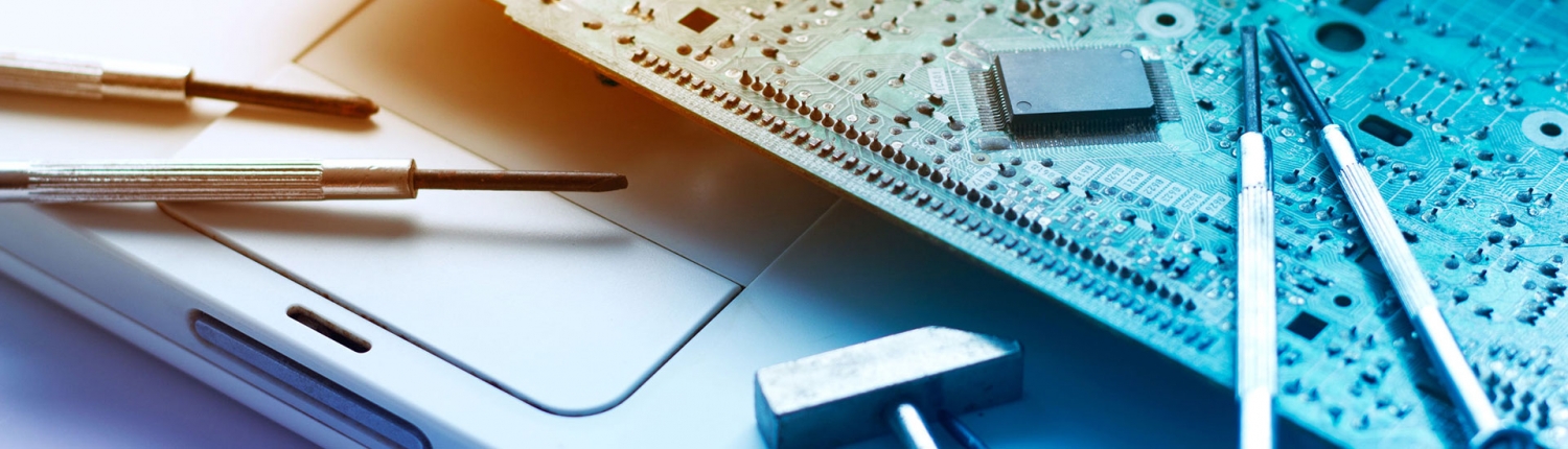


PCB Layout
Whatever your application, in portable electronics, computers, test equipment, manufacturing, optics or spacecraft, Elik-tronics can develop your PCBs to streamline your digital, analog, mixed-signal, high-speed, RF and wireless components, from design to manufacturing.
With our in-house team we can take care of the whole process. Thanks to cooperation with a Chinese factory, we can create high-quality PCBs up to 30 layers, for any and every of your objectives, delivering on time and within budget, for prices that are reasonable. We will take care of furnishing you with the essential documentation, while we advise you on each of the design steps and possible strategies. We can do the pre-production verification, perform final checks, and make your transition to manufacturing as smooth as possible.
Along the design to manufacturing cycle we will advise you about trade-offs, routing yields, operating margins, alternate devices, optimization, trace impedance, and the best choice for SI (signal integrity). Together we are committed to finding you the best balance between performance, cost and manufacturability.